JEDEC Approves SPHBM4: Next-Gen AI Memory with 300% Faster Per-Pin Speed, 80% Fewer Pins
The relentless demand for AI compute has pushed high-bandwidth memory to its limits — not just in speed, but in the sheer complexity and cost of packaging it alongside processors. The international semiconductor standards body JEDEC has now answered with a significant architectural pivot: SPHBM4, a new standard that promises to untangle the packaging knot while preserving — and in some respects exceeding — the performance of today’s HBM4.
Designated JESD330-4, the standard was developed by JEDEC’s DRAM committee JC-42.2 and has now received final approval from the board of directors. At its core, SPHBM4 addresses a fundamental pain point of the HBM ecosystem: the reliance on interposers, advanced substrates, and intricate packaging techniques that drive up manufacturing costs for GPUs, AI accelerators, and HPC chips, while also constraining production capacity.
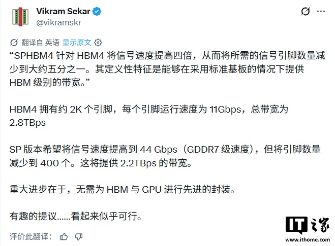
The numbers tell a striking story. Today’s HBM4 implementations typically feature around 2,000 signal pins running at approximately 11 Gbps each, yielding a total bandwidth of 2.8 terabytes per second. SPHBM4 radically rethinks this approach. By using standard substrates and eliminating the need for complex packaging, the new standard reduces the signal pin count to roughly 400 — just one-fifth of the HBM4 baseline.
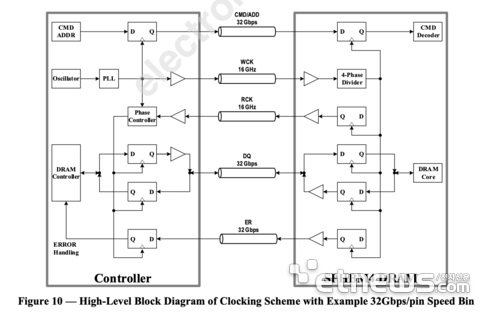
To compensate and maintain competitive bandwidth, SPHBM4 quadruples the per-pin data rate to roughly 44 Gbps. The result is a memory interface that delivers near-HBM4-class bandwidth through a far leaner, more manufacturable physical layer. Fewer pins and standard packaging mean lower cost, simpler integration, and — crucially — the potential for higher-volume production at a time when AI chip supply chains are under intense strain.
The implications for the AI hardware landscape are significant. By decoupling high-bandwidth memory performance from exotic packaging requirements, SPHBM4 opens the door for a broader range of chip designers to integrate competitive memory subsystems without the prohibitive cost and supply constraints of advanced packaging. This could accelerate the proliferation of purpose-built AI accelerators and democratize access to high-performance memory architecture.
JEDEC’s move comes as the semiconductor industry grapples with the “memory wall” — the growing gap between compute throughput and the ability to feed data to processors fast enough. SPHBM4 represents not just an incremental upgrade, but a strategic rebalancing of the trade-offs between signal count, speed, and packaging complexity that have defined the HBM era.